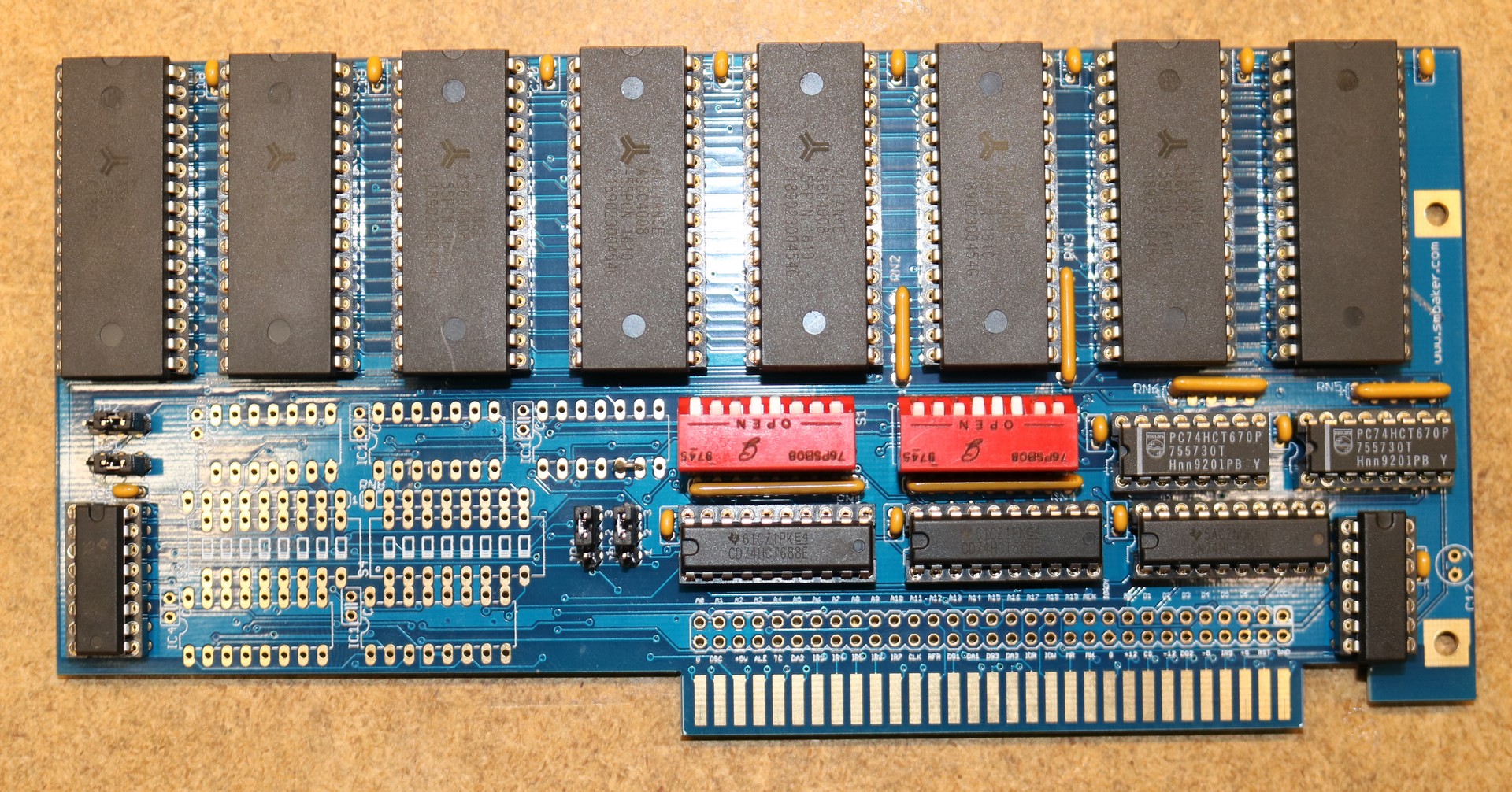
In this post, I create an 8-bit ISA board that can be used either as expanded memory (EMS) or as a flash disk:
Motivation
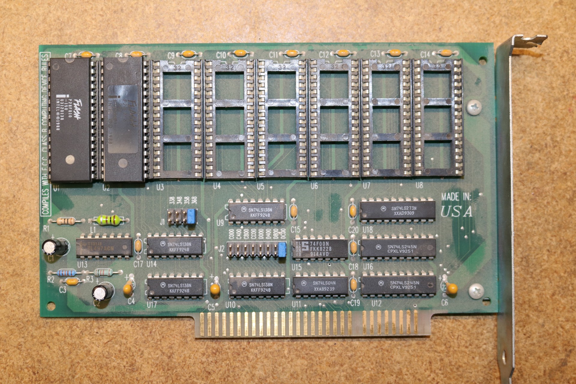
The motivation for this project came from a Boca Start Card that I owned back in the late 80s or early 90s. The Boca Start Card was one of the first PC solid state disks. It used 28F010 Flash chips that were 128 kilobytes each. There were eight sockets, which allowed for up to 1 megabyte of flash storage. The most I ever owned was two flash chips (they were expensive back then!) so my Boca Start Card had 256 KB of storage space. That was enough flash to hold DOS, network drivers, and whatever else was necessary to boot one of the nodes of my BBS. Whereas the alternative at the time would have been to boot from floppy or hard drive, this allowed a solid-state no-moving-parts scenario.
There were a few limitations to the Boca Start Card. For example, it only supported up to 1 Megabyte of space, which isn’t a lot. The disk could only be written to using a special command-line tool, which I had occasional reliability issues with. It uses an older flash technology that requires high voltage (12V) to program and is only capable of whole-chip erase, not sector erase. As a challenge, I decided to implement my own flash drive.
Early in the design process, I realized that an expanded memory system and a flash storage system can be implemented in almost exactly the same way. The only difference is the type of memory device used and the write behavior. Static RAM (SRAM) used for an EMS board can be written one byte at a time, but isn’t persistent. Flash must be written a sector at a time (4KB) and is persistent. So I decided to include in the design the ability to configure the board as either Flash or EMS.
The basics of memory paging
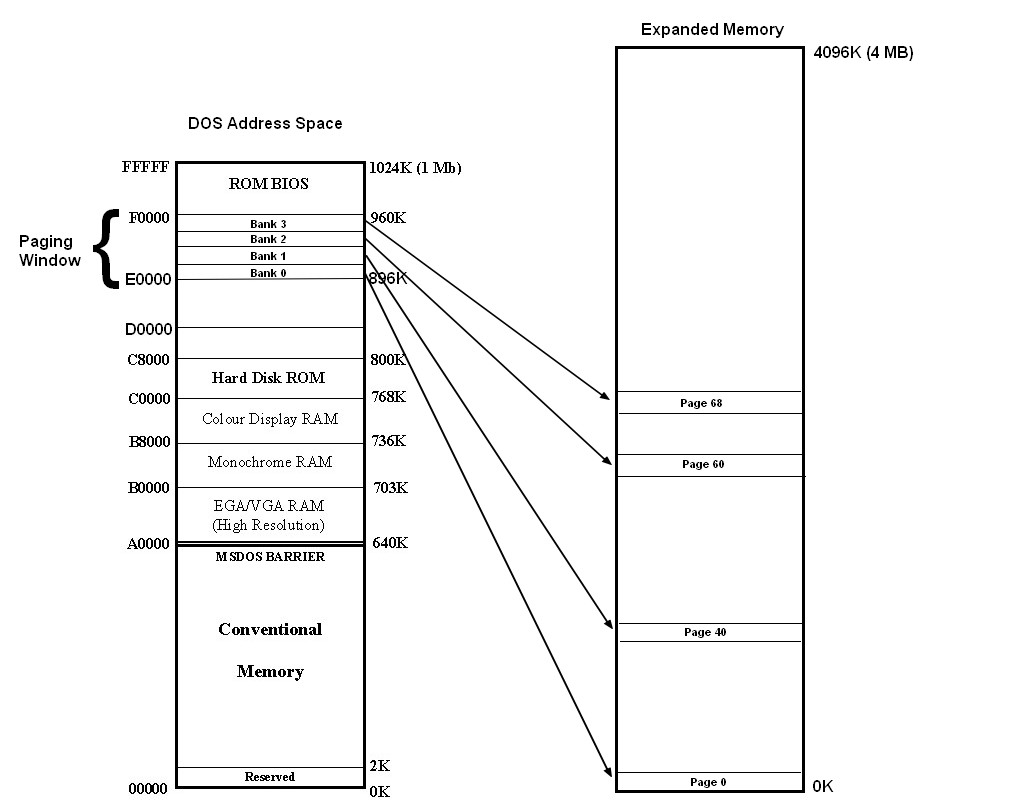
The 8088 only has 20 bits of address space, which corresponds to 1 Megabyte of addressable space. Much of this (~ 640KB) is taken up by conventional memory, which holds running programs. Other portions of the address space are taken up by BIOS ROMs, video memory, etc. So how to we expand this relatively limited space to allow additional memory to be added? The answer is to use a hardware paging scheme.
We designate a window, typically 64KB, typically at 0xE0000, in the CPUs address space that we will map various pages into. We break this window into four 16 KB banks. By using some hardware translation, we will use a set of page registers to allow you to map any of these four banks to a 16 KB page of external memory. The advantage of this approach is that we can now address more than the CPU’s limited 1 megabyte of storage space, but the disadvantage is that we have a limited window into that space. We can only “see” up to 64KB of the banked memory at a time. If we want to look at different portions of the space, then we need to adjust the page registers.
Design
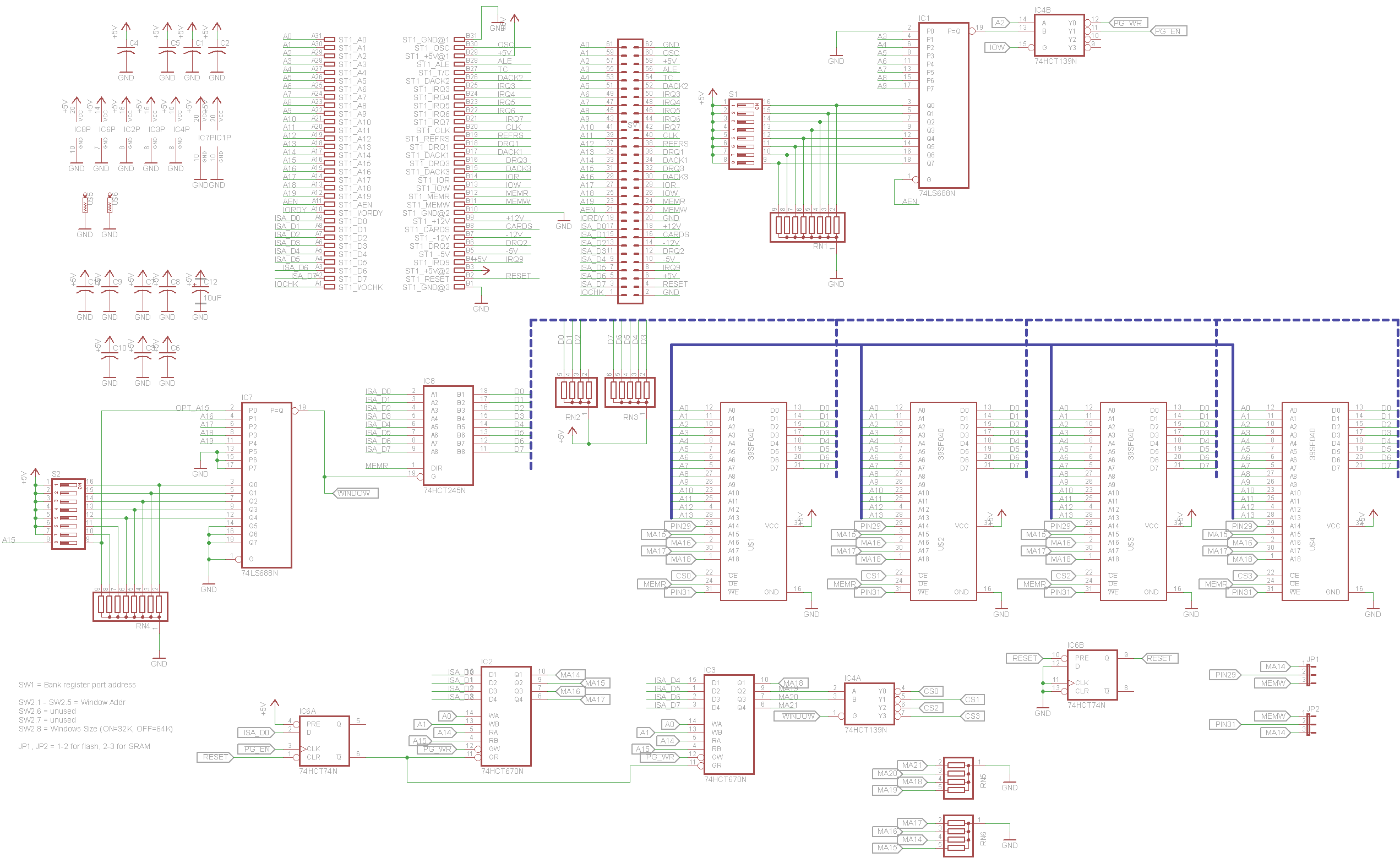
The schematic is shown below.
The basic paging system is borrowed from Sergey Kiselev’s Zeta-2 design. We use a pair of 74HCT670 register file chips to hold the page registers. Each 74HCT670 has four addresses that can be independently read and written, and each address holds four bits. Using two chips gives us four addresses that can hold eight bits of data per addresses. These four addresses in the register file correspond to the four banks that can be selected in the page window. Since each register is 8 bits wide, the registers can store 256 different values. That gives us 256 possible pages that we can map. 256 * 16 KB = 4 MB of pageable address space. We could conceivably add a third 74HCT670 register file and expand the size of the page register to 12 bits, giving us a fantastically large amount of mappable memory, but we really don’t need to on an 8088 PC as software of that era didn’t really expect to find much more memory.
The nice thing about the 74HCT670 register file is that it has independent read and write mechanisms. You can write to the page registers using one set of pins (WA/WB to select the address, GW to write, D1-D4 for data) and then read using a different set of pins (RA/RB to select the address, GR to read, Q1-Q4 for data).
You’ll note there are two different dipswitch-74HCT688 address decoder blocks in the schematic. One of these is used to select the address of the memory window, typically set to 0xE0000. The other address decoder is used to select the address of the page registers, typically at 260h. A program writes 8-bit values to the page registers at 260h – 263h to configure paging, then it reads and/or writes memory at 0xE0000 – 0xEFFFF in order to use that memory.
Five bits of the page register is directly applied to the upper five address lines (A14-A18) on the memory ICs, selecting a 16KB page within the IC. The remaining three page register bits can be used to select which memory IC to use. In the 4-IC version of the Flash/EMS board, I use a 74HCT139 2-4 decoder to allow four chip selects. In the 8-IC version of the Flash/EMS board, I use a 74HCT138 3-8 decoder to allow eight chip selects.
The 39SF040 Flash Memory ICs and AS6C4008 Static RAM ICs have an almost identical pinout. It’s annoying that they’re so close and yet slightly far away. The Flash devices use pin 31 for Write, whereas the SRAM devices use pin29 for Write. This necessitated adding some jumpers, JP1 and JP2. Jumper pins 1&2 to configure as flash, or pins 2&3 to configure as SRAM.
There’s one last wrinkle to consider and that’s the page-enable logic. When configuring this board as Expanded Memory (EMS), it doesn’t matter what state the page registers are in when the computer is booted, since the EMS driver will soon take control of the page registers. However, if the board is configured as Flash storage, then we want to make sure that each time the computer is booted, the page registers all point to page 0, so we can locate a BIOS extension there. For this reason we use a 74HCT74 flip-flop that is cleared on reset, and set on a page-enable write.
Implementation
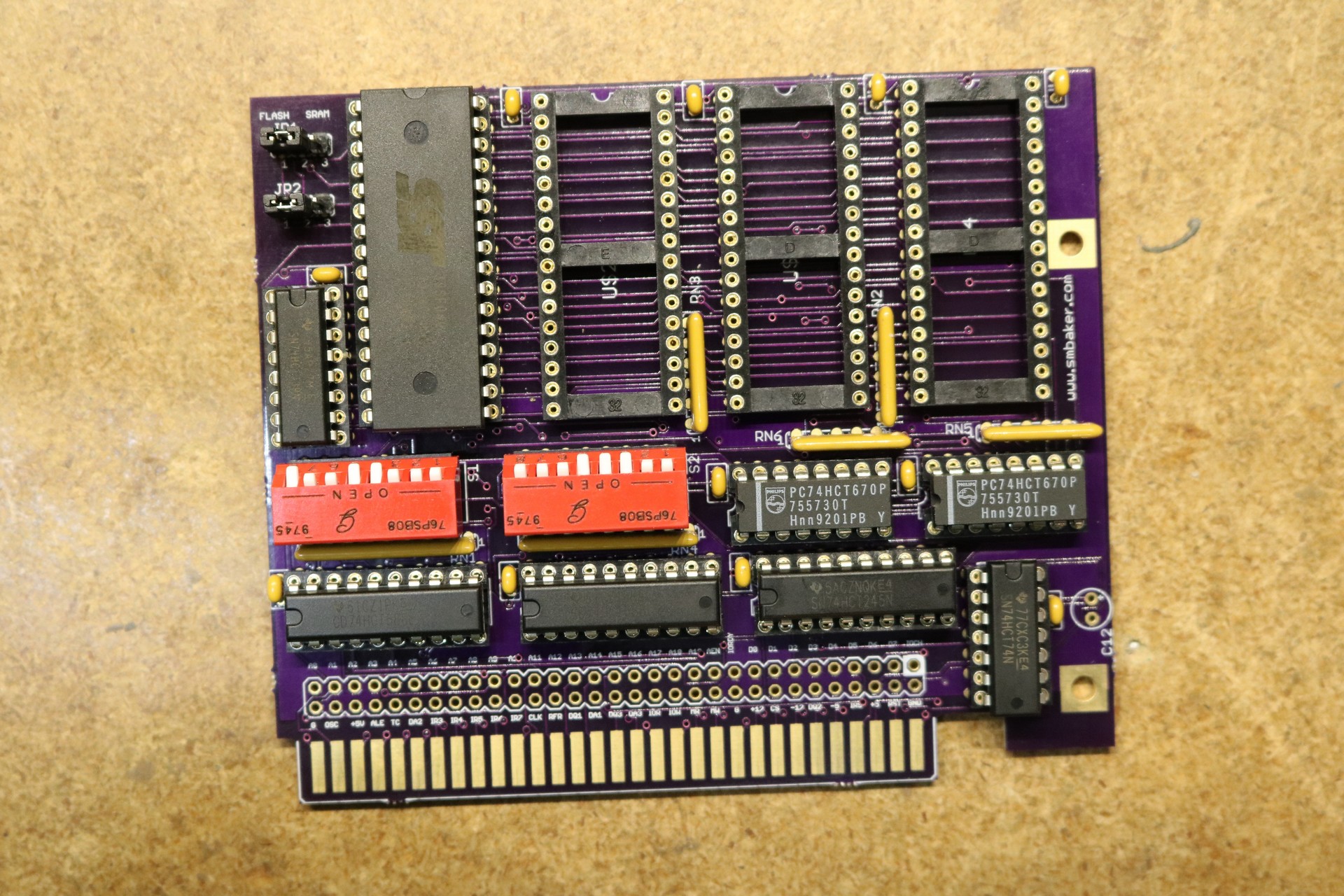
I had some boards fabricated. The four-IC version I fabricated at Osh Park, like usual:
However, the larger 8-IC board would have been cost prohibitive at Osh Park, so I had it fabricated using Seeed Studio’s fusion PCB service:
Implementation of the 4-IC board is identical to the schematic.
Implementation of the 8-IC board … well … that’s up in the air. I found that stability was adversely affected as I continued to add more memory devices. The system was stable at four memory devices, but became progressively worse as more were added, becoming more-or-less unusable at 8 devices. Bummer. It was such a nice looking board, too. 🙁 The problem was traced down to issues with the address bus, and I suspect adding address buffers will resolve it.
The EMS Driver
The popular Lo-Tech EMS Board included a driver, with source code, that works almost out-of-the-box with the 4-IC board when configured as EMS. The “almost” comes from my page enable logic. The way I implemented the 4-IC board, you have to write a 1 to port 0x264 to enable paging. This required me to update the Lo-Tech driver to support my board. Instructions for patching the driver are included at my github repo.
For the 8-IC board, I did away with the need to write an enable bit, allowing any write to the page registers to serve as an enable. However, the Lo-Tech driver only supports 128 pages, and the 8-IC board provides 256 pages, so the driver had to be modified to support the 8-IC board as well.
The Flash BIOS
When configuring the board as a flash device, instead of the EMS driver, I wrote a Flash BIOS extension that makes the board look like a floppy disk. The BIOS extension hooks BIOS int 13h, which serves as the BIOS disk handler. Reading data is fairly simple — we do some math to convert the Cylinder, Head, and Sector of the read request into a block address within the flash memory space. Then we set the page registers so the appropriate page is mapped in. Finally we execute a loop that transfers a 512 byte sector from flash to the user’s buffer.
Writing flash is a whole lot more complicated than reading it. Unfortunately, you can’t write a byte at a time, you have to first erase and then write an entire Flash “sector”, which on the 39SF040 is 4096 bytes in size. BIOS sectors are 512 bytes in size. This means we have to allocate some conventional memory to serve as a temporary sector buffer. Whenever a write occurs, we do the following:
- Copy 4KB from Flash to the temporary buffer
- Copy the 512KB write request to the temporary buffer
- Erase the 4KB Flash sector
- Write 4KB from the temporary buffer to Flash
Unfortunately, using my naive implementation, this means that any time you write a 512B sector, a full 4096B write needs to be performed. Since there are eight 512B bios sectors in a 4096B flash sector this means that a sequential file write is generally inefficient by a factor of eight. My bios extension could be modified to be smarter about this, deferring writes until a whole 4096B sector was ready to be written at once, but that’s more work than what I want to go to at this time…
One the subject of writing flash, it’s not quite so simple as a “REP MOVSW” like it is in the read case. After the erase is completed, each byte needs to be written individually using a special write sequence (see the 39SF040) data sheet. Basically, what this all means is that when using my Flash BIOS extension, you want writes to be really rare. Basically my intent is to use it as a read-only filesystem, with the occasional write when something needs to be tweaked.
Board Ordering
Resources

This is excellent, and I can’t wait for the buffered address 8 chip version. I was wondering if your code for the floppy emulation is available somewhere?
Hello Scott,
any info on the 5 pin and 6 pin resistor networks values? These are not the standard resistor networks for the dip switches, usually 10KOhm. These are pull ups and pull downs for some data bits etc. Thanks. It would be wiser in your project to put the values of the components!
Regards.
Additionally it is not clear the orientation of the dip switches. On the silkscreen they are upside down, because probably you defined to use a 90° dipswitch facing up. So the PIN 1 is on the left. But using a standard dip switch the orientation on the silkscreen is reverted. I mounted a standard dip switch with position 1 on the left and position 8 on the right, but now the address bits are reversed in the dip switch. The orientation of the dip switches should be more consistent in your projects. Also on other boards you put the silkscreen in reversed orientation, but on the videos/pictures they are soldered reversed. So it’s a mess to understand the relative pin vs address bit. Additionally. it should be nice to have dip switch meanings on the silkscreen (eventually the back).
Where can I find the gerber file for this board?
I wish some body would do a EMS board for the DEC Rb100 computer that used the memory expansion connector. It would be a little more complex, many because any I/O cards that did use the Memory Expansion connector switched RAM and BIOS ROM overlays On and Off. On a hardware interrupt the EMS boards overlay RAM Memory is switch off and the BIOS ROM is active. At the Return form Interrupt the EMS RAM bank is turned back on. The systems memory map is also different (, up to 896K of RAM possible).
Companies like Sealevel want to much to make a few boards and I had no luck with Lo-Tech.uk.
Hi. I made a board following your wonderful project, but I can’t get the driver. I got the lo-tech driver and patched it with the file you posted, but it keeps failing. Maybe the lo-tech driver has been updated in the meantime, could you please send me the driver for my do-it-yourself board? Thank you. rorirori6969@naver.com
You’ve somehow solved the above problem!
Fortunately, it compiled successfully on my DOS box.
But should I use 104 for C1 to C11?
I’d also like to know the values for RN1 through RN6. Is it okay to use 10kR?
Thank you for sharing this. I am presently in need of an LIM EMS 4.0 Expansion Board. I am reseaching any that suit my needs and considering designing my own.
Question for you: This uses the Lo-Tech EMS driver, am I to take it that this is LIM EMS 3.0 implimentation?
Cheers,
Matt