In this post, I create an ISA card that can serve as either a DiskOnChip board, or a RTC, or both:
Background
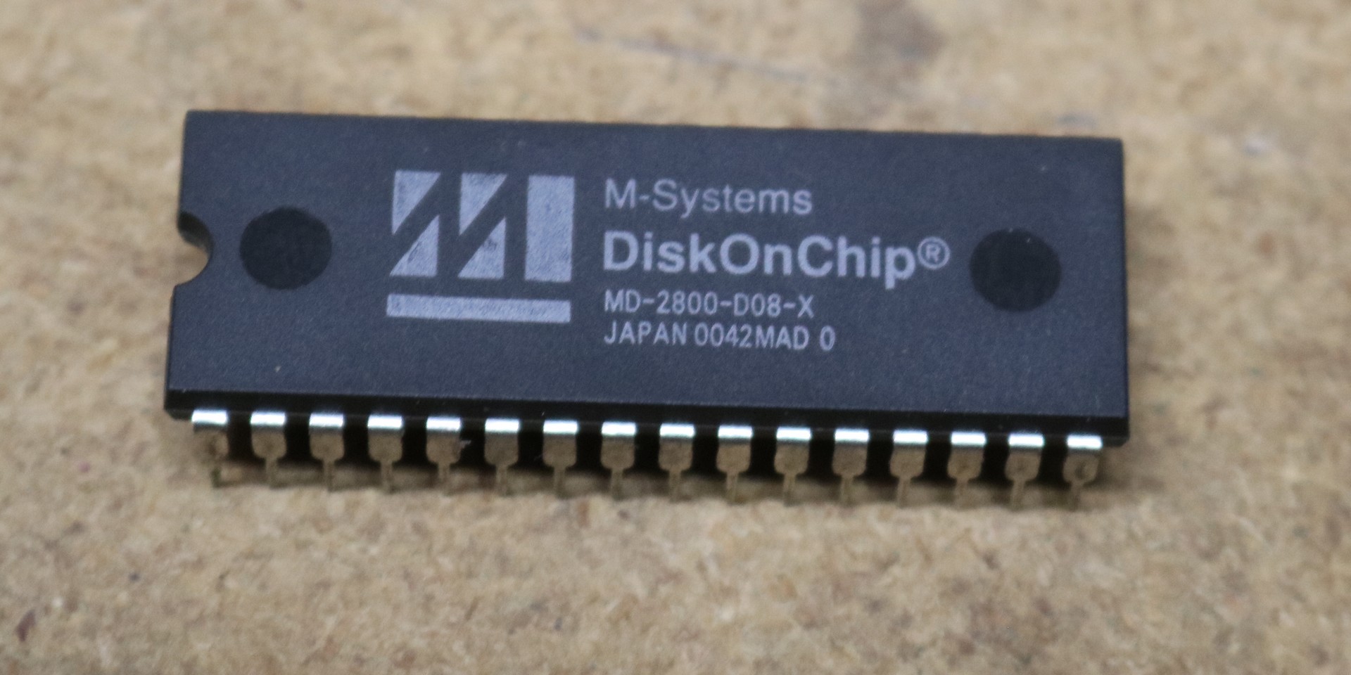
DiskOnChip is a series of products manufactured by m-systems in the 90s and 2000s. There are several versions available, from standard 32-pin DIP IC packages, to IDE interface versions. This post is going to discuss the IC version. Here is a used sample that I attained from eBay:
I’ve already built a couple of other flash storage devices, such as my Flash/EMS board that offered up to 4 megabytes of storage using 39SF040 flash devices. The DiskOnChip is yet another step in my exploration of flash storage devices.
The advantage of the DiskOnChip IC is that it combines the flash storage and controller in a simple IC package that is compatible with common memory pinouts. Versions of the DiskOnChip are available from 8MB up to 384MB in size, which would have been significant back in the 1990s and 2000s. The DiskOnChip does this while only using an 8 KB memory window into the processor’s address space, making it particularly attractive for computers with limited address space such as the early x86 computers (IBM PC, XT, etc). The logic for paging the flash into the window is all incorporated into the DiskOnChip IC.
Design
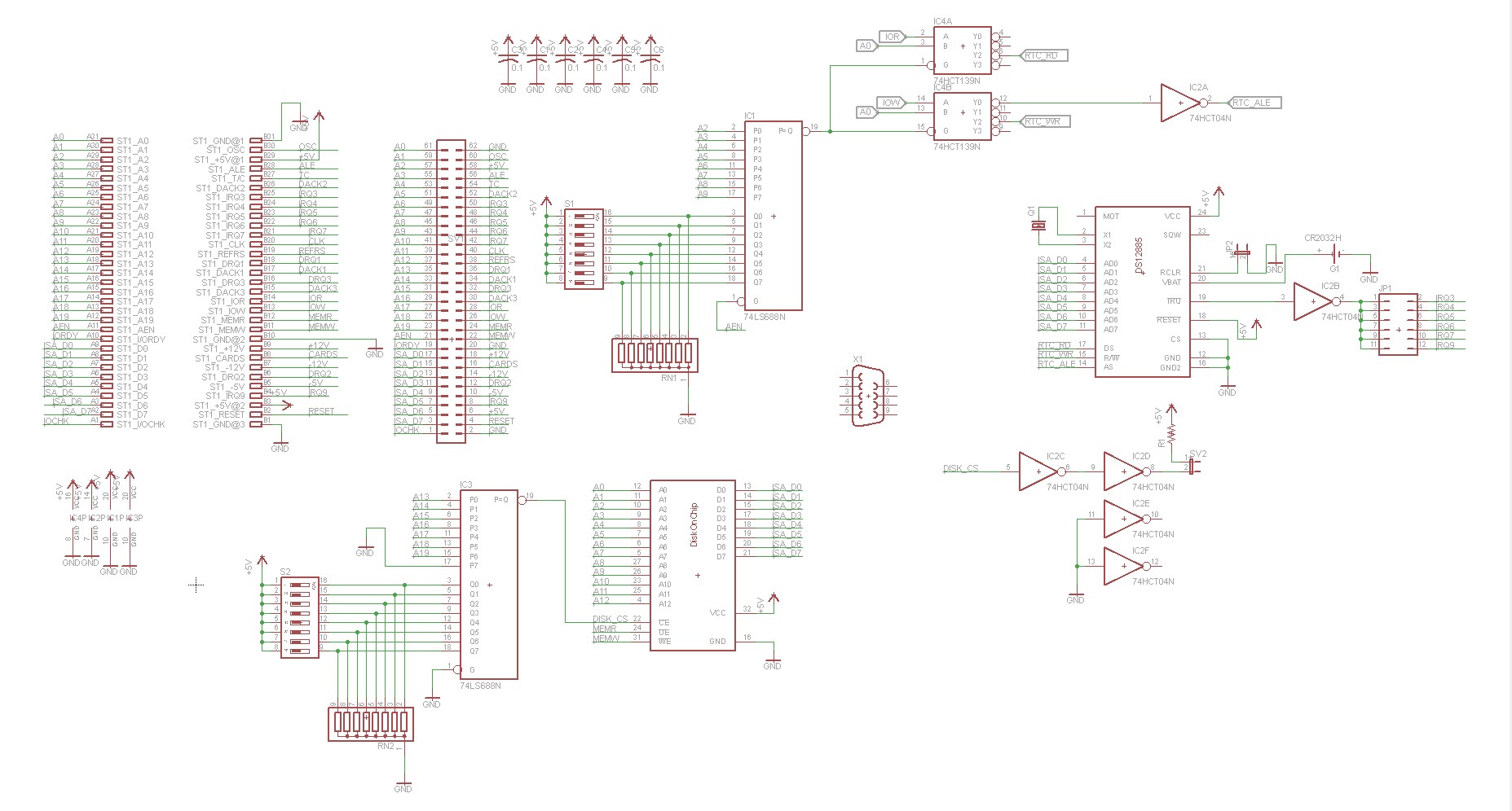
Here is my schematic:
As you can probably tell, there’s multiple things going on with this design. I had extra room on the board, so I incorporated both a real-time clock (RTC) as well as the DiskOnChip. Don’t worry, the circuits are entirely separable. The only parts required for the DiskOnChip are the DiskOnChip IC and its associated decoding logic, consisting of a 74HCT688 magnitude comparator, pullups, and dip switch.
The 74HCT688 has two 8-bit sets of inputs, and outputs a low whenever the two sets of inputs match. Typically one set of inputs goes to a set of dip switches and the other set of inputs goes to a set of address lines. When the address lines match the dip switches, the chip select is asserted. As the DiskOnChip uses an 8KB window into the address space, 13 address lines are used for that 8KB window leaving 7 address lines remaining (A13-A19) for the 74HCT688. This allows us to place the DiskOnChip at any 8KB boundary in main memory. Typically I put it at 0xE0000.
As only 7 address lines were used, that left one input remaining on the 74HCT688. I grounded P7 while leaving Q7 connected to the dipswitch. This means if the dipswitch connected to Q7 is set high, than the DiskOnChip is not addressable. This is handy to allow you to prevent the DiskOnChip’s onboard BIOS extension from being invoked at boot time (say, for example, if there was a problem with the BIOS extension that prevented boot).
Implementation
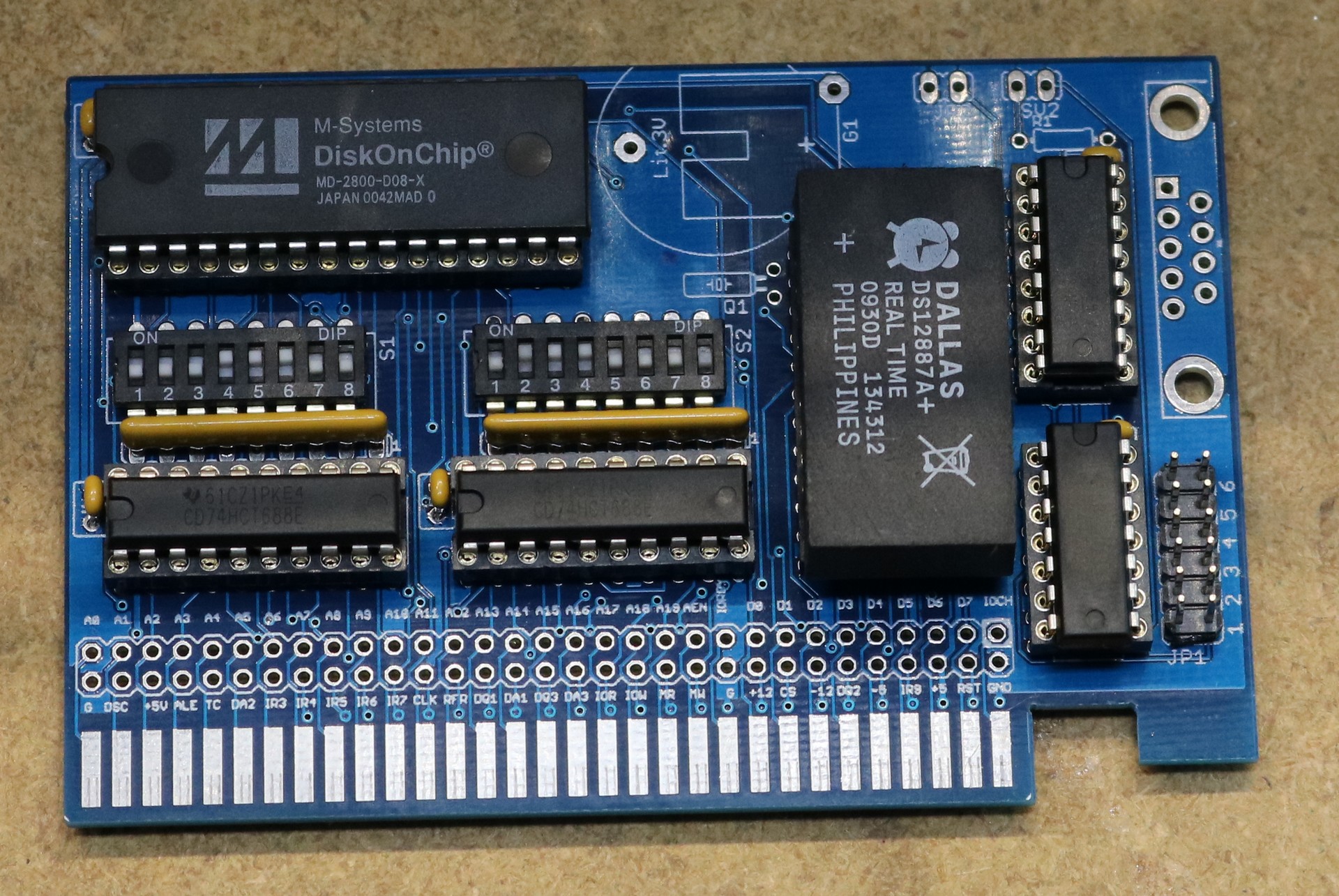
I had boards fabricated at OSH Park:
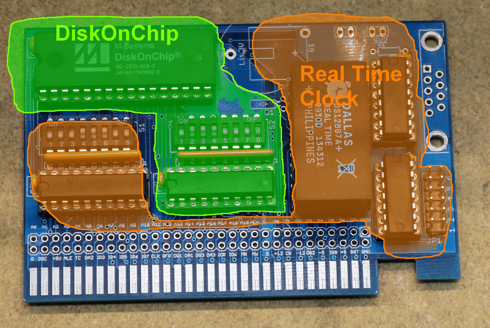
To make it a little bit clearer how the board implements the DiskOnChip and Clock functionality, here is an annotated diagram:
Only the components necessary for the particular function need be implemented. You can implement both if you want, as the DiskOnChip and RTC have independent address decoders.
Board Availability
As usual the boards can be found at Osh Park:
On the Osh Park board page there is a download link that will allow you to download gerbers.


Hi Scott
Where can I find the DOS software for this board?
How can I download the Gerbers from OSH Park, I see there a download button, but I get only a XML file.
Regards
Thomas
@Thomas Reisen: You need to download EagleCAD, the free version and generate the gerber files from the .brd file, which is an XML file, that you downloaded from OSH Park.
Hi,
What is the resistor network ohm value, that is, the yellow component on the board connected to the dip switches for the disk IC?
The schematics does not say.
Thanks
The resistor network should be 10k. It’s often the case that the value of a pullup/pulldown is not very critical — anything in the neighborhood ought to work.
Hello,
Sorry to disturb you, I am trying to assemble the board. Can you tell me what are the characteristics of the resistor arrays you are using ? And what is the use of the pin header on the right side (JP1)?
Thank you
Seems I didn’t jot down the values in the schematic, and I don’t have the board in front of me to check, but I would expect 10K to work. Looking at my schematic, I see two headers — SV2 and JP2. JP2 is to clear CMOS memory. SV2 is for an optional activity LED (I don’t think I ever tested an activity LED; the associated R1 resistor goes along with it).
Hello,
Thanks for the explanations. Can you tell me what the values and type of the 3 capacitors? Is there any bill of materials available somewhere?
Have a nice day,
It does not work with XT motherboard if there is no HHD controller or as in your case there is XTIDE BIOS loaded.
So better was to combine DiskOnChip module with XTIDE bios on one ISA board … and this will work on all XT boards than.
But now you have to plug HDD controller , even without disk , to be able to use the disk.
Another comment. The dip switches for the interrupt selection have standard 1, 2, 3, 4, 5, 6 positions on the silkscreen. It would have been wiser to write the relative interrupt number. The projects of Sergey Kiselev are always magnifically documented and silkscreens are self explanatory. Your projects, for someone not very expert, require an additional long time to understand some basic information so we must gather (or guess, looking at the schematics), missing informations. But dipswitch configuration and components values like resistors, condensers, resistor networks, are always missin.
Hi Scott
Where can I find the DOS software for RTC?
Does this board design support the MD2200 series chips i looked at the data sheet for both and they have the same pinouts.
Where I can find all possible dip-switch positions per adress?
Can I change schematic so that I can see active DOM? I think that I must replace SV2 through a LED. Is it correct?
Can anyone manage to bring the RTC to life?
Yes, me!
I took a few days to look at the circuits. Now it is already clear to me how it works, both parts work well for me.
Scott,
In your video, you mentioned that you needed to rebuild the bootloader to work with your 8088. Do you (or can you) make any of this available? Any special tools you needed to create?
As usually ends up happening, I was planning this same thing to add fixed disk storage to a Sharp PC4502 and stumbled on your project (I somehow always seem to be following you in ideas a few years later!) This PC4502 is also a V40 based computer.
Thanks for all you do!