In this post, I interface a vacuum fluorescent display to the RC2014:
Sourcing displays
These vacuum fluorescent display modules can be found easily on ebay, just search for “Noritake VFD”. They’re available in a variety of different configurations from single line displays to four line displays. A word of caution about the larger displays — some of them, such as 4×40, do not offer the “8080 mode” that I used in this blog post and will require different interfacing techniques.
The VFD modules will typically include a jumper on the back that selected between “68” mode and “80” mode. For the purposes of this blog post, we want to operate in 80 mode. Every one of these modules I’ve seen has had this jumper unbridged, so you’ll need to bridge it, either by soldering across the jumper or by installing a two pin header and a shunting block.
VFD Board Design
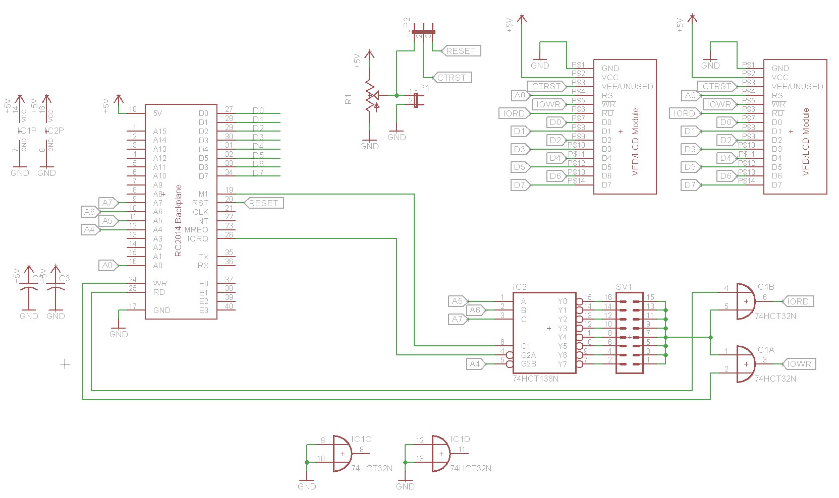
Here’s a schematic of the VFD display board:
You’ll notice that there are two VFD modules shown in the schematic. One is a 1×14 SIP header footprint, and the other is a 2×7 SIP header footprint. The Noritake modules you find on eBay will typically be one of the other.
I included a potentiometer for contrast control. This isn’t used for VFD displays, but may be useful for LCD displays (many LCD displays use the same pinout as these Noritake modules).
We have the same 74HCT138N decoder logic that I used for most of my other RC2014 compatible peripheral boards. There’s also a 74HCT32N OR gate, that’s used to combine the RD signal with the CS signal, and the WR signal with the CS signal to generate IORD and IOWR signals. That’s what the Noritake module will expect when operating in 8080 mode.
VFD Board Implementation
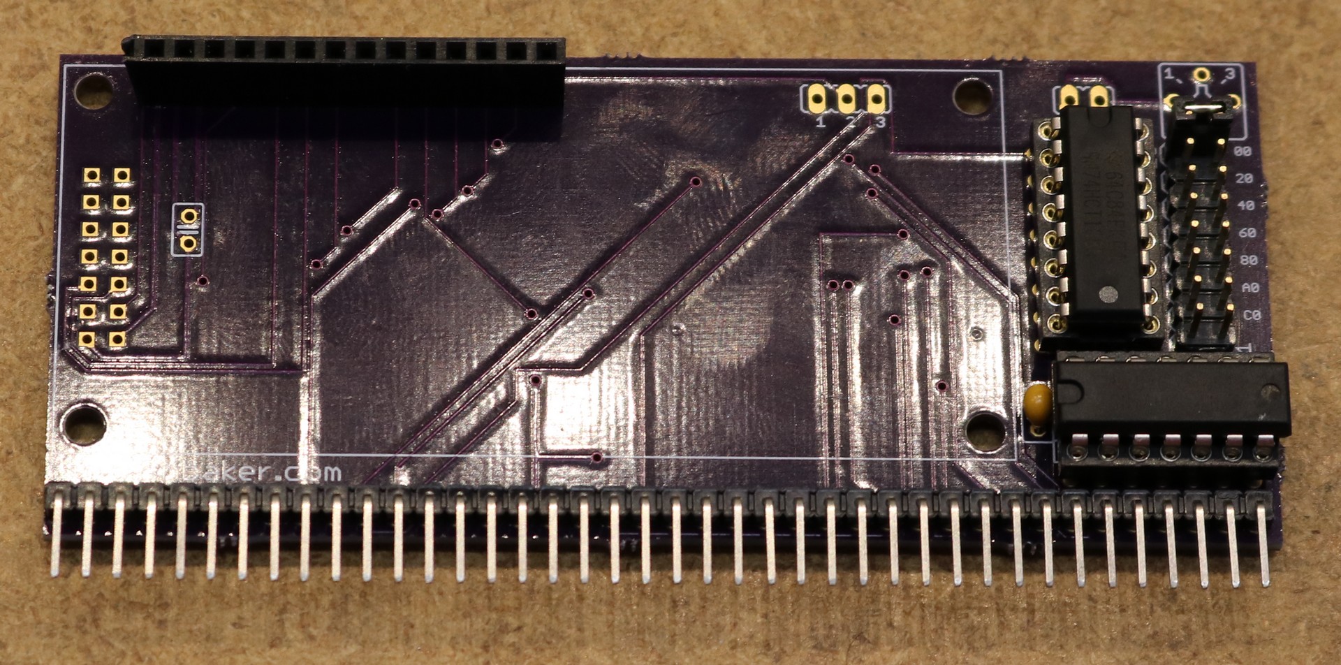
Here’s the completed board:
Revision 0.5
I’ve revised the VFD display boards to accommodate larger displays like the Noritake 40×4, featured in my CP/M and Unix videos. The revised board is also available on Osh Park. It uses an additional 74HCT138 to provide chip selects for the additional drivers on the larger VFD module.
Bill of materials (revsion 0.1)
- PCB, Osh-Park
- 1×14 or 2×7 female 0.100″ header
- 2×8 male 0.100″ header
- 74HCT138N
- 74HCT32N
- 0.1uF capacitor
- 40-pin right angle SIP header
- IC sockets as desired
Bill of materials (revision 0.5)
- Revision 0.5 PCB, Osh-Park
- All the parts in revision 0.1
- One additional 74HCT138N
- Two 1×3 male 0.100 headers
- Two additional 2×8 male 0.100 headers
PC-Board Ordering
As usual, I’ve made the board available on Osh Park:
Revision 0.1 Board:
Revision 0.5 Board:


Would a 40×4 HD44780 compatible LCD work with your VFD variant of RomWBW? I’ve got one in my parts box that I’m sure would look great displaying CP/M.
Also, many thanks for sharing your hard work. I’ve got a few of your boards now and they add so much to the RC2014.
I was curious if you have an updated schematic for the revision 0.5 board. I not sure what JP3 and JP4 are for? I am not using the optional IC3 chip at the moment. I am using the smaller of the two VFD’s and am using the Rev 0.5 board exactly the same as the Rev 0.1 Board with the address selected at 00 per your video.
Once again. This is a fantastic post!