In this video, I build a new Flash ROM / RAM board and use it to install the RomWBW CP/M distribution on the RC2014:
I’ve already done one video on CP/M on the RC2014, but when I built the Zeta 2 Single Board Computer, I liked Sergey Kiselev’s design so much that I thought I’d try to adapt it over to the RC2014.
Overview of the new design
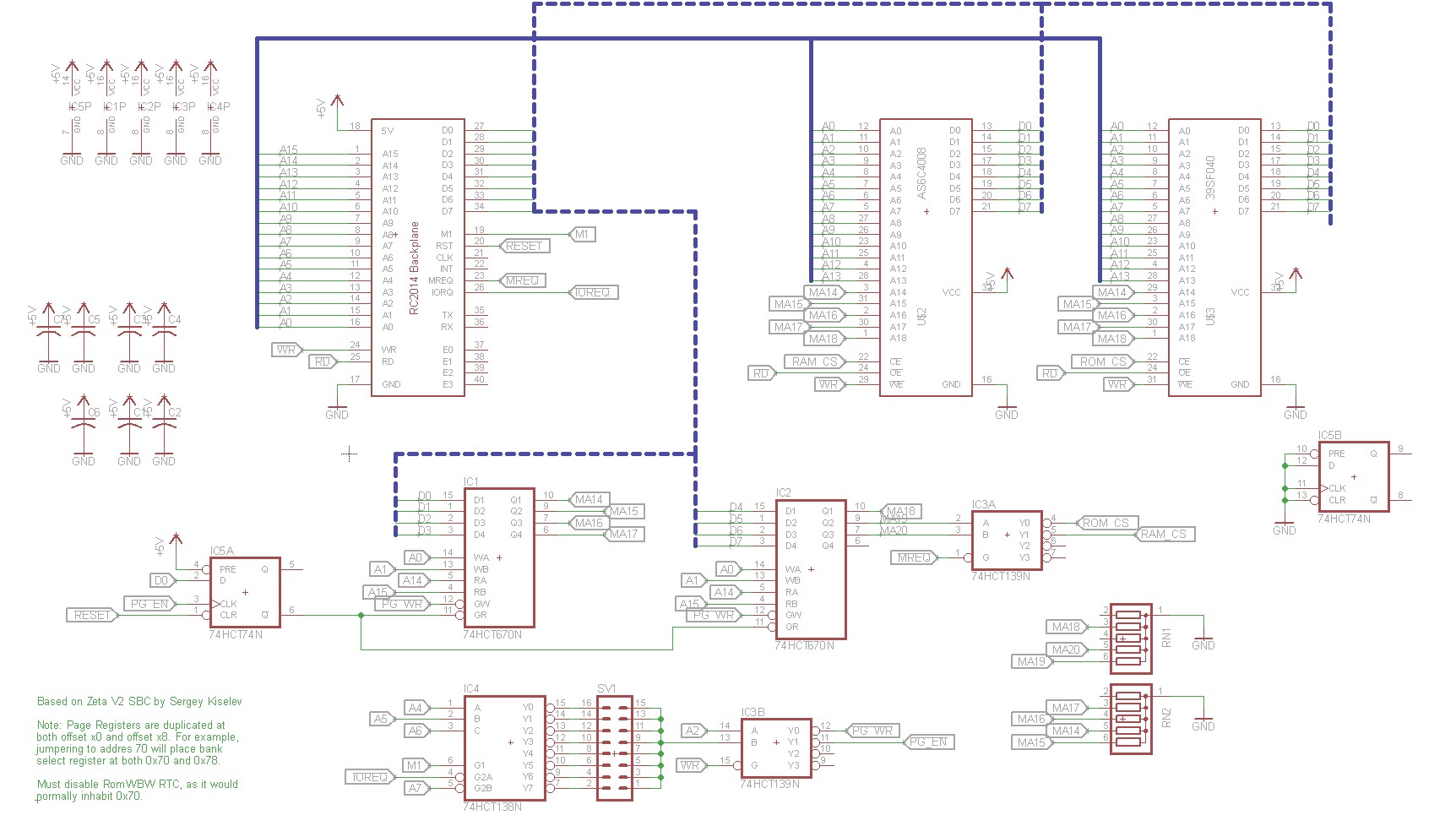
The new design, based on the Zeta 2 by Serget Kislev, uses a 512 KB Flash ROM and a 512 KB static RAM. There are two register file chips that implement a 7-bit paging register. This allows you to slice up the Z80’s 64 KB address space into four windows, each of which can point to any 16 KB page in ROM or RAM.
There are several advantages to the new design:
- The CP/M operating system and BIOS is built into ROM
- ROM disk allows over a dozen CP/M applications and tools
- RAM disk allows programs to be downloaded, assembled, etc.
- No external storage (CompactFlash or Floppy) is needed for a basic CP/M system
- Flash ROM can be reprogrammed without needing to be erased
Schematic
Here’s a picture of the schematic
Implementation
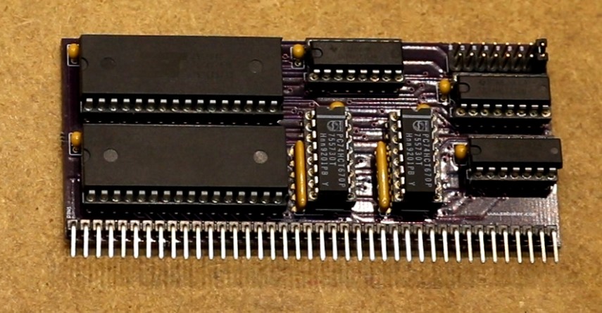
Here’s the board I built
Modifying RomWBW
The CP/M distribution that runs on the Zeta 2 is called RomWBW by Wayne Warthen. Since the RC2014 is not exactly a Zeta2, I had to make a few modifications:
- Added support for the Z80 SIO/2 chip
- Added support for the ICAI chip (for those using the original RC2014 serial board)
Github makes it very easy to fork an existing project and make available your own changes. My fork of RomWBW is located at https://github.com/sbelectronics/RomWBW
Flash ROM / RAM Board Bill of Materials
| Name | Description | Supplier |
|---|---|---|
| Pc-board | osh park | |
| U$2 | 512K Static Ram AS6C4008 | digikey 1450-1027-ND |
| U$3 | 512K Flash ROM 39SF040 | digikey SST39SF040-70-4C-PHE-ND |
| IC1, IC2 | 74HCT670N register file | ebay or digikey 296-33164-5-ND |
| IC3 | 74HCT139N dual 2-4 decoder | digikey 296-8390-5-ND |
| IC4 | 74HCT138N 3-8 decoder | digikey 296-1608-5-ND |
| IC5 | 74HCT74N dual flip-flop | digikey 296-1625-5-ND |
| SV1 | 2×8 male header | |
| RN1, RN2 | 10K x 5 (6-pin) resistor network | digikey 4606X-1-103LF-ND |
Board Ordering
As usual, the boards are up on osh park:


Scott,
Absolutely great!! Thank you for sharing your work.
My Zeta SBC V2 is under construction, but I would
like to expand my RC2014 with your board. Hope
you will share this on OSHPARK or the Gerber files.
Maybe you will share also a version of the Flash
BIN image.
Thomas
Hi Dr.Scott,
Nice project ! Interested in your case design for RC2014. Can you share the design ? Can you please tell me where can I order the case ? Thank You.
Yes, I’ll see about getting the files checked in…
Scott
Dr.Scott,
Thank you for the reply. I also interested about the 4×40 vfd display that you implemented. I see that you have share the board at oshpark. Is there any BOM info
for the board (for the 4-line displays footprint that
you have added) ? Can you share the documentation about
the serial console mirroring part to the vfd display ?
Thank You.
Masayuki
Many thanks for this great project. I thought before I build the hardware that I would get an Eprom programmed so went through the build cycles – all to the video and all went OK, just a question at the BUILDROM.cmd stage – I get the same options as you – so selected SMB but options that then come up are different – I get acia, acia_vfd, SIO, SIO_vfd, SIO_vfd_8in ….. I selected SIO but do you think this will be a problem (I didn’t get the ‘std’ that you selected). Thanks for your advice
I changed the options to allow people to build for different hardware. The “SIO” option will build for the SIO/2 board that I had configured in my RC2014 in the video. The “ACIA” option will build for a 68B50 ACIA (the RC2014’s original serial board). Assuming you are also building the SIO/2 board, then you chose correctly.
This is a great board, can we have an explanation of the “SV1” header and the purpose of the jumper connections?
Thanks again,
Mark
SV1 selects the address the page registers are at. You can select any of eight addresses — 00, 10, 20, 30, 40, 50, 60, and 70. The registers will appear twice within the address range. Jumpering to 70 will place the page register at 70 and 78, and the page enable register at 74 and 7C. For compatibility with RomWBW, you would want to jumper it to 70, as RomWBW expects the page register at 78 and the page enable at 7C.
Hi, Scott –
It is so satisfying when a project goes together and works the first time it powers up! Mine was built with the original RC2014 ACIA serial port. It is kind of cool that Wayne’s RomWBW has both CP/M and ZSDOS built in. Many thanks for all the hard work you put in getting all the hardware working! Now, on to the WDC floppy card tomorrow.
Jim
Hi Scott, ROMWbW working great on CP/M and standard cfg (ACIA)- have now built SIO/2 pcb only (not the RTC) and burnt the SIO/2 eeprom. when I power up I get the standard boot screen but when I type a command e.g ‘C’ nothing happens. I’ve scoped the RX signal right onto the RC14 bus and it’s there OK, therefore is there something I’m missing? Do I need to tie any of the SIO/2 ports down on Port B? or any other links with no RTB?
Many thanks for any help…
Colin
Is the second SIO port available for use under this implementation of RomWBW?