In this post, I add a Z80 CTC (counter-timer) and SIO/2 (serial IO) to the RC2014
If you haven’t read my other Z80 retrocomputing blog posts yet, then please start with the first one, Intro to Z80 Retrocomputing, for an overview of the RC2014 platform.
Motivation
All I wanted to do was connect a GPS module to the RC2014… This turned out to be much more difficult than I anticipated.
I started by designing a dual 68B50 serial board, but I neglected to pay attention that the GPS module I chose (UP501) operated by default at 9600 baud. While you can configure it to operate at additional baud rates, you have to send the configuration command at the power-up default, which is 9600 baud. The 68B50 can be configured with a clock divider of 1, 16, or 64. With the RC2014’s system clock, that allows us to easily select 115,200 baud by using a divider of 64. However, there’s no way to easily select a baud rate that is less than 115,200 baud.
I explored a number of alternatives to adding additional clock chips and dividers. This seemed like a lot of work and special-purpose complication, especially if I wanted to be able to control the baud rate using software. Ultimately I decided to use the Z80 CTC. The CTC offers 4 independent counter/timers. Three of them have external outputs, which we can connect to our serial chip to use as a baud rate reference.
68B50 vs SIO/2
My original solution was a dual 68B50 board. For whatever reason, this proved very unreliable. It was sensitive to which slot it was plugged into the RC2014 backplane. It had to be right next to the CPU, or occasionally it would do weird things like drop characters or fail to reset properly. I spent a fair amount of time trying to debug my dual 68B50 board, and ultimately decided on using the SIO/2 instead.
The SIO/2 is a dual serial chip. It is far more complex than the 68B50, offering different operating modes and fancier interrupt support. For configuration there are eight different write registers and three different read registers. One advantage is that one SIO/2 chip yields two serial ports, whereas I would have needed two 68B50.
CTC Board Design and Implementation
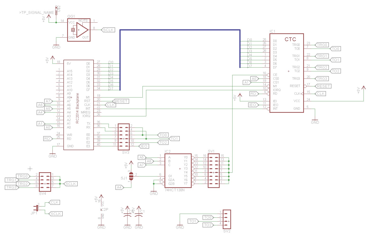
Here is the schematic of the CTC board
The schematic is fairly straightforward. There’s a 74HJCT138N for address decoding, which is used as a chip select for the CTC. I’ve brought the CTC’s signals out to a couple of places. TO0, TO1, and TO2 (the outputs) are brought out to a header at the top of the board and to some jumpers that let you easily connect them to the RC2014 backplane’s extra pins. TRG0, TRG1, TRG2, and TRG3 (the triggers) are brought out to a dual pin header block that allows you to easily connect them to either an on-board oscillator or (if the on-board oscillator is not installed) to the system clock. SJ1 is a jumper that allows you to restrict addressing to when A4 is high. This will let you put the board at 10,30,50,70,90,B0,D0 instead of on 00,20,40,60,80,A0,C0,E0 like my other boards. My plan is to put the board at 0x90 so that it shares the 0x80-0x9F address range with the SIO.
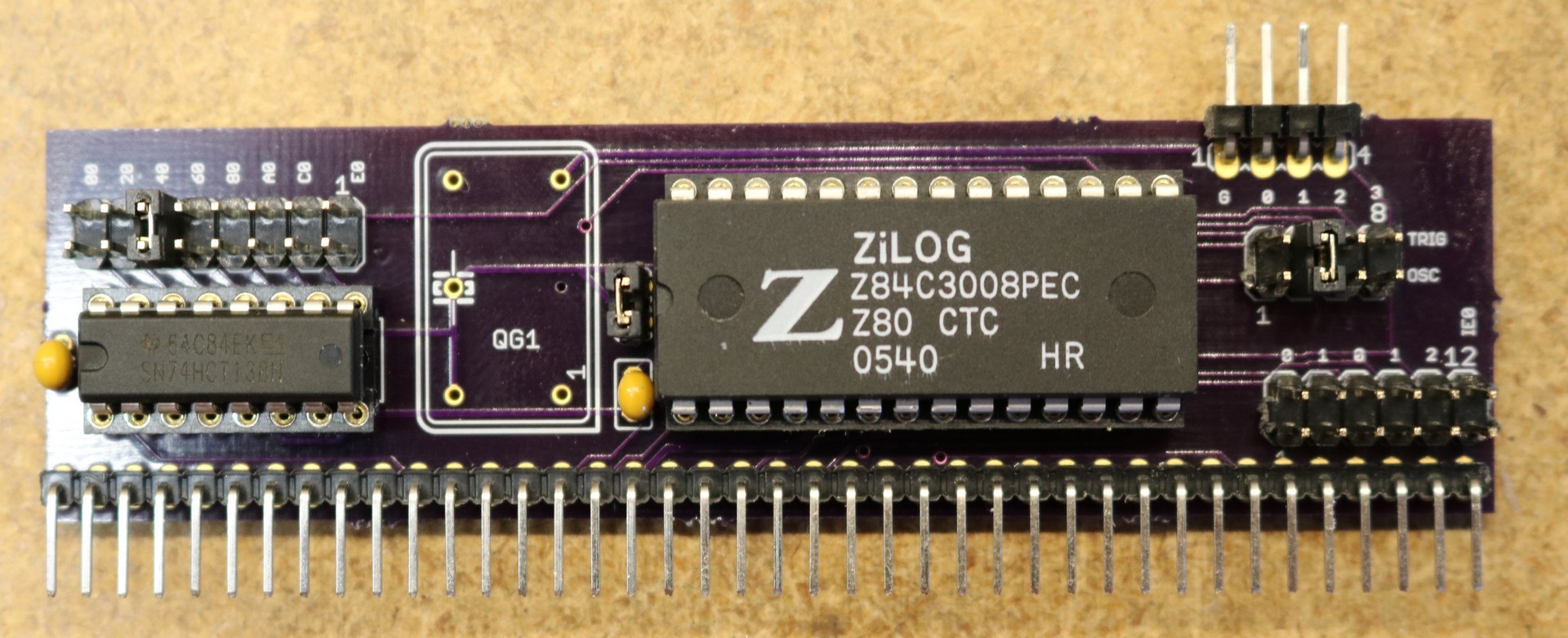
Here is my completed CTC board:
As you can see, I’ve left the footprint for the crystal unpopulated. The jumper to the right of the crystal footprint passes the system clock over to the TRIG/OSC jumper block to the right of the CTC chip, where I’ve jumpered it to the channel 1 trigger.
SIO Board Design and implementation
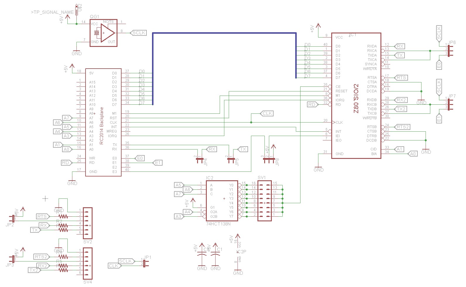
Here is the schematic of the SIO board:
This is also a fairly straightforward board. We again have a 74HCT138N for address decoding that allows us to put the board on 00,20,40,60,80,A0,C0, or E0. The serial ports are brought out to a pair of 6-pin headers that allow you to easily connect FTDI cables or other devices like a GPS. I opted not to install a MAX232 driver on-board. If you really want a 9-pin serial port, then a MAX232 can be installed externally.
There are two jumpers, JP6 and JP7 that allow you to either select the system clock as the clock source, or get clock from one of the RC2014 backplane’s extra pins. The idea is that a CTC pin will be brought out to E1 on the CTC board, and then picked up on E1 for the SIO board to allow us to set custom baud rates. The TX and RX pins can be jumpered to the backplane as well. Finally, there is a jumper for the interrupt mode that allows you to either use 5V (interrupts allowed all the time) or to connect the interrupt pin to E3, where it could in theory be connected to the CTC board. For simple implementation, I enable the interrupts all the time, but the CTC and SIO do have a more sophisticated mechanism where they can generate interrupt vectors that identify the device that generated the interrupt.
There is an optional oscillator footprint that allows you to use a custom oscillator, and a jumper to use the system clock instead of the custom oscillator.
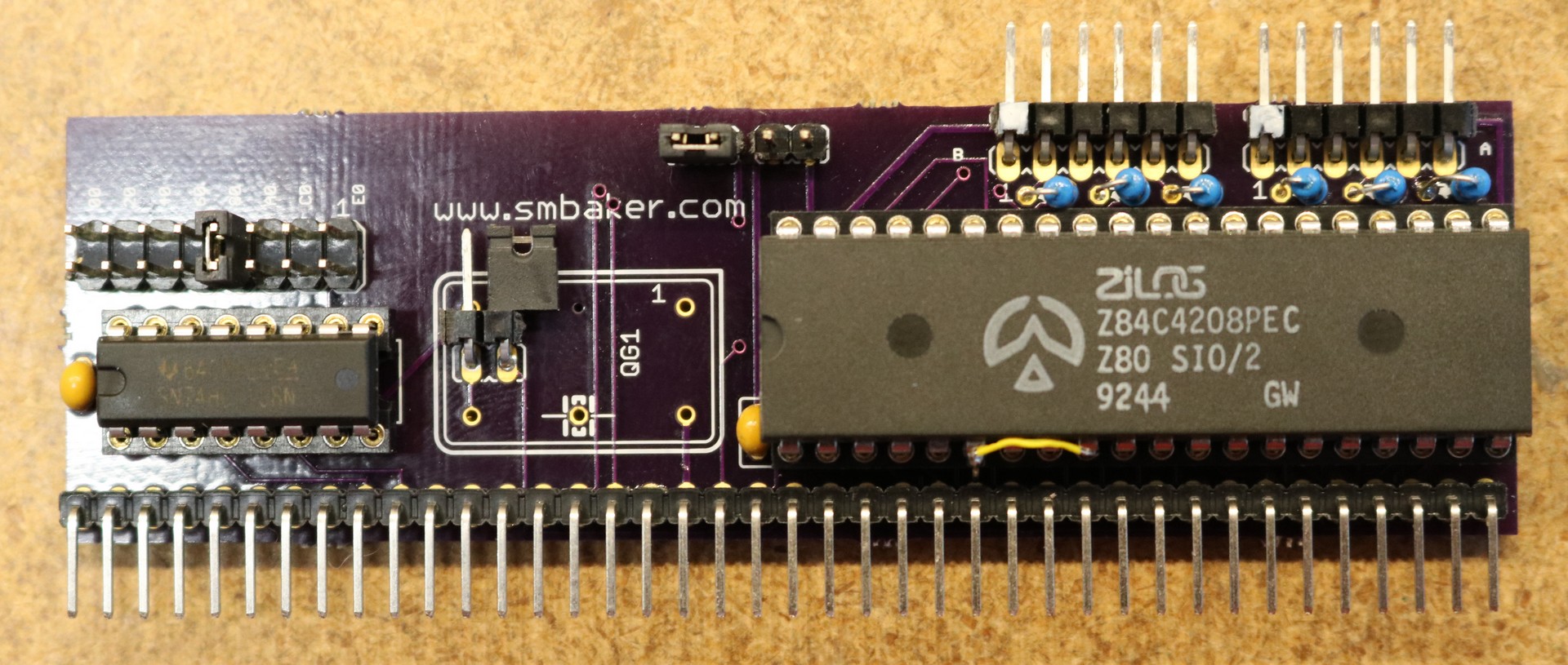
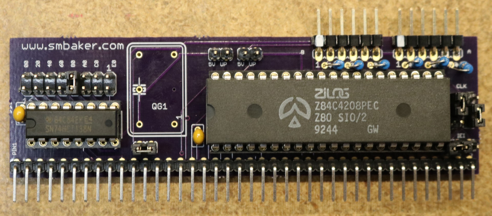
Here is the completed board:
As you can see, this board has a few … imperfections … I mistakenly wired the IEI pin to GND when it should have been wired to 5V, hence the yellow jumper wire. I also didn’t have any provisions for using separate clocks for ports A and B (not visible, but there is a cut trace under the SIO chip and a piece of yellow wire on the back to deal with this). These issues have been corrected in the schematic, and I’ll soon be sending off for a replacement board.
Here is the revised version:
As you can see the revised one fixes the hacked in piece of yellow wire, and adds three new jumpers. The two jumpers on the very right side of the board are the clocks for Ports A and B (note the order is A then B, whereas the order of the port headers on the top of the board is B then A). Immediately beneath the clock jumpers is a jumper marked IEI which selects the source of the IEI pin. If fits a little tight next to the SIO chip, but it does fit. You can either select IEI from 5V to fix the interrupts as enabled, or jumper it to the fourth spare pin on the RC2014 backplane. This board revision is the one that is available on the Osh Park link at the bottom of this page.
The way I have the board jumpered in the picture above is:
- address 80h
- port A clock = clock from RC2014 backplane
- port B clock = second extra pin on RC2014 backplane (which is in turn supplied by CTC chip)
Programming the CTC as a baud rate generator for the SIO/2
My first attempt was to use the CTC in timer mode. This seemed relatively simple to me, I would take the system clock, prescale by either 256 or 16, and then setup the time constant for the final division to yield the appropriate baud rate. The SIO/2 would be configured to divide by 1. Here are my calculations:
CPU Frequency = 7,372,800 Hz.
| Baud | Prescaler | Time Constant |
|---|---|---|
| 1200 | 256 | 24 |
| 2400 | 16 | 192 |
| 9600 | 16 | 48 |
| 19200 | 16 | 24 |
| 38400 | 16 | 12 |
| 57600 | 16 | 8 |
| 115200 | 16 | 4 |
Unfortunately, the above scheme didn’t work very well. Sometimes it would work, but sometimes the SIO/2 would end up out of sync with the incoming serial stream and output occasional splotches of gibberish. After some experimentation, I found that my SIO/2 was unreliable whenever the clock mode was set to X1. The same thing would happen when I tried to use my 68B50 with an X1 clock divider. I’m still a little bit confused at this; my reading of the data sheets led me to believe this would work just fine. Maybe it comes down to quality of implementation and my PCB layouts aren’t quite clean enough for the X1 mode.
I did find that the SIO/2 would work perfectly if the clock mode was set to X16. This means we have to output a rate from the CTC that is 16 times higher than our baud rate. For a baud rate of 115,200 that would mean outputting a timer rate of 1,843,200 Hz. Since the CTC always selects a prescaler (either 16 or 256) in timer mode, a 7.3728 MHz system clock is insufficient to produce a timer rate of 1,843,200 Hz.
This led me to try operating the CTC in counter mode with an external trigger. Counter mode works much like timer mode, but it counts external pulses via the trigger input. The advantage to counter mode is that the X16/X256 prescaler is not forced upon you. We can feed the system clock into the trigger input, and then use timer mode to output the baud rate we want.
| Baud | Timer Rate | Time Constant |
|---|---|---|
| 1200 | 19200 | 96 |
| 2400 | 38400 | 48 |
| 9600 | 153600 | 24 |
| 19200 | 307200 | 12 |
| 38400 | 614400 | 6 |
| 57600 | 921600 | 4 |
| 115200 | 1843200 | 2 |
This worked perfectly. I was able to read from my GPS without constant weird splotches of high-ascii gibberish.
If you check my math in the above table, you’ll notice the time constants are half of what you’d expect them to be. This surprised me, and I think I found the answer in the CTC data sheet: “Although there is no setup time requirement between the triggering edge of the External clock and the rising edge of Φ (Clock), the down-counter is not decremented until the following pulse“. Since I have the trigger connected to the system clock, it’s counting every other trigger pulse.
Modifying RC2014 Basic
I started with Grant Searle’s Z80 SBC modifications to Nascom Basic. A link to Grant Searle’s ZIP file containing source code is here. The changes I made are the following:
- Use an SIO/2 instead of a 68B50
- Modify interrupt handler, TX, and RX functions for the second serial port.
- Add a BAUD rate function to set the baud rate.
- Add four new BASIC keywords: ISER, OSER, RSER, and BAUD.
The new basic keywords function as follows:
- ISER(x) – read a character from serial port (x=0 or 1)
- RSER(x) – check readiness of serial port (x=0 or 1)
- OSER x,y – output character Y to serial port X (x=0 or 1)
- BAUD x,y – set baud rate on port X to Y (x=0 or 1, y=1 for 1200, 2 for 2400, 9 for 9600, 115 for 115200)
Here is a sample program that reads all characters on the second serial port and writes them to the first serial port.
10 REM check port 1
20 IF RSER(1)=0 GOTO 50
30 X=ISER(1)
40 OSER 0,X
50 GOTO 10
Wiring it all up
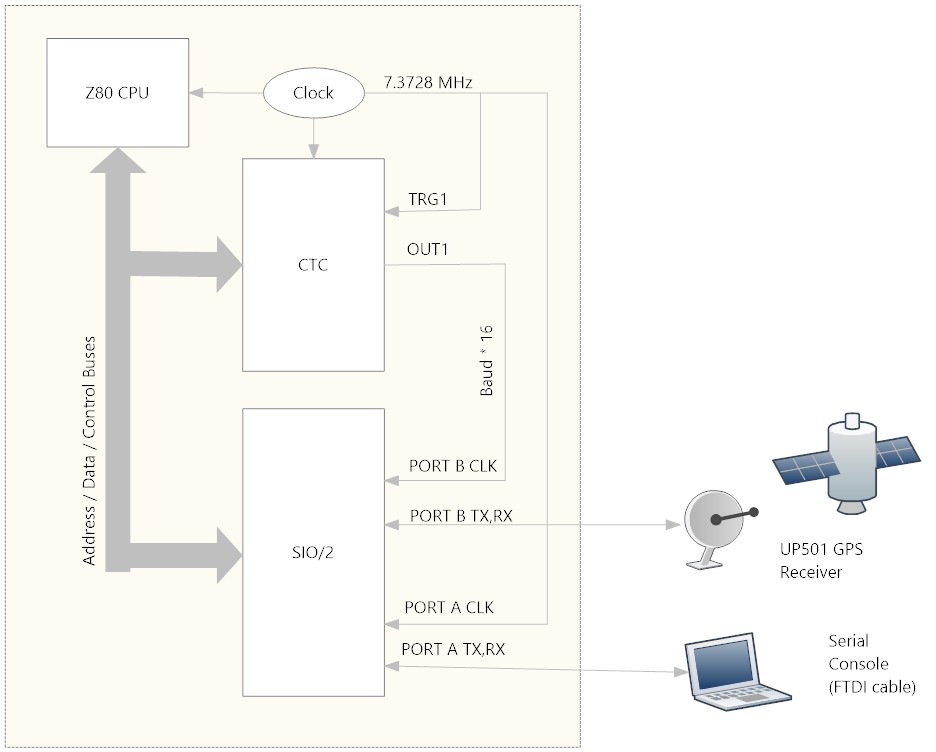
Here’s a diagram of how everything is connected:
Source code
As usual you can find the source code in my github repo at http://www.github.com/sbelectronics.
Bill of Materials
SIO/2 board
| Name | Description | Supplier |
|---|---|---|
| pc-board | Osh Park | |
| R1-R6 | 2.2k resistor | |
| C1,C8 | 0.1uF capacitor | |
| IC1 | Z80 SIO/2 Z84C4208PEC | eBay |
| IC2 | 74HCT138N 3-8 Decoder | |
| QG1 | Crystal oscillator, optional |
CTC board
| Name | Description | Supplier |
|---|---|---|
| pc-board | Osh Park | |
| C1,C8 | 0.1uF capacitor | |
| IC1 | Z80 CTC Z84C3008PEC | eBay |
| IC2 | 74HCT138N 3-8 Decoder | |
| QG1 | Crystal oscillator, optional |
PC-Board ordering:
As usual, you can find them on osh park:
CTC Board
SIO/2 Board


Hi Scott
Love your site and your youtube videos. Thanks for sharing
I wondered whether you are planning on uploading the designs for your SIO and CTC boards to OshPark?
Thanks
Rob
Yes, I’ll be sharing the designs soon. The CTC board design is good. The SIO I had to revise due to a few errors.
Hi Scott, Fixed the problems with OSH Park! My order for 5 of your boards in one go seemed to glitch the website. Jenner fixed and I am waiting for them to arrive. Already gone to FAB so hopefully should here in the UK in short time.
I think there may be a typo in the Programming the CTC as a baud rate generator section above. in the 4th para you say
…This led me to try operating the SIO/2 in counter mode with an external trigger. … should this not be CTC?
Best Regards
Paul
Yes, that looks like a typo. Thanks. I’ll fix!
Scott
Sir,
I was curious what the resistor values are for the SIO/2 board.I did not see this on the schematic. I purchased a copy this the board from OSH park and have the parts.I assume the Caps is the standard. My RC2014 is up and running and researching your wonderful projects.I am looking forward to getting CP/M working. Great work!
Hi Scott,
These look well very attractive, well thought out, and understandable with just a little study. Today I ordered a set of your CTC and SIO/2 boards from OshPark, along with some of your other RC2014 boards. I’m really looking forward to building them and coding drivers for them.
Two questions: 1) What are the resistor values on the SIO board? 2) Do you anticipate any problems if I use a 7.3728 Mhz oscillator on the SIO board instead of using the RC2014’s system clock — in particular do you expect there would be problems if the system clock and SIO’s separate clock ran at different speeds or were not exactly in sync with each other?
Thanks!
Oops… For my second question I meant to ask about putting the oscillator on the CTC, not on the SIO. That question should read:
2) Do you anticipate any problems if I use a 7.3728 Mhz oscillator on the CTC board instead of using the RC2014’s system clock — in particular do you expect there would be problems if the system clock and CTC’s separate clock ran at different speeds or were not exactly in sync with each other?
I don’t think there would be an issue, that’s one of the reasons why I added a crystal footprint to the board (as well as the SIO/2 board), though I haven’t used it myself. Please let us know how it turns out!
Resistor values are 2.2K.
The resistor values are 2.2K. The capacitors should be standard 0.1uF bypass caps.
The 1x clock mode was also erratic for me. Switching to counter mode and then 16x multiplier on the SIO did work stable.
Why the 1x clock mode doesn’t work I think:
The datasheet says:
“If the x1 clock mode is selected, bit synchronization must be accomplished externally. ”
I think this is what the problem is: The clock is only as fast as the baud rate. To read in the middle of the bit we need an edge in the middle of the bit. The CTC doesn’t provide a falling edge in the middle because it’s duty cycle is less than 5%. That falling edge for read sometimes coincide with an edge of the signal. With 16 ticks, it’s easy to read in the middle of the bit.
If you take a look at the Z80 Peripherals Guide (http://www.z80.info/zip/um0081.pdf) page 235 (PDF page 255) under the heading “Asynchronous Receive” you’ll find the answer to the mystery of why the 1x clock divisor mode didn’t work reliably for you.
Like any asynchronous receiver, in order to reliably synchronize the bit timing at the start (and within the sequence) of a frame (start bit, data bits, parity, stop bit(s)), the SIO needs to sample the state of the receive data line at multiple of the bit rate. With the clock divisor set to 16, the sample rate is 16 times the bit rate — i.e. a full bit time is 16 clocks. When the receiver sees a transition to logic 0 for the beginning of a start bit, it doesn’t consider it to be start bit unless it stays at logic 0 for half a bit time — with the divisor set to 16, that’s 8 clocks. After the receiver is sure that it saw a start bit, then the “center” of each of the following bits will occur at intervals that are 16 clocks in length.
If the divisor is set to 1 (as noted in the document), you are obliged to include additional logic in the circuit to the synchronize to the start of each “frame” and fire clocks at the appropriate times to reliably read the state of each bit.
Absent the frame-to-frame synchronization that occurs when the receiver’s sample rate is a multiple of the bit rate, or some external logic to do the synchronization when the receiver’s sample rate is equal to the bit rate, it cannot work reliably.